
Addressing Challenges in LED Driver PCB Layout Design
- April 26, 2023
- Posted by: Admin
- Categories: Device Engineering, Internet of Things
LED lighting’s popularity has increased due to its energy efficiency and longer lifespan than traditional lighting, highlighting the importance of LED driver design.
However, addressing a number of challenges is necessary to ensure optimal performance and reliability while designing the LED driver circuit for these lighting systems.
Designing the PCB layout carefully is one of the key challenges in LED driver design to minimize thermal issues, EMI, noise, and other potential problems that could impact the circuit’s performance.
To create high-quality and reliable LED driver circuits, it is essential to understand the requirements of the LED driver circuit and how to design the PCB layout to meet these requirements.
This article will explore the key considerations for successful LED driver PCB layout design, including managing thermal issues, minimizing EMI and noise, designing for manufacturability, selecting the right components, and leveraging simulation tools.
- What is LED Driver PCB Layout Design?
- How to Overcome the Challenges in LED Driver PCB Layout Design?
- Understanding the LED Driver Circuit Requirements
- Strategies for Managing Thermal Issues in LED Driver PCB Layouts
- Minimizing EMI and Noise in LED Driver PCB Layouts: Best Practices
- Designing for Manufacturability: Tips for LED Driver PCB Layouts
- Selecting Components for LED Driver PCB Layouts: Key Considerations
- The Power of Simulation Tools for Successful LED Driver PCB Layout Design
- Wrapping Up
What is LED Driver PCB Layout Design?
An LED driver PCB layout design is the process of designing the printed circuit board (PCB) layout for an LED driver circuit.
The LED driver circuit is responsible for providing power to the LEDs, controlling their brightness, and regulating their current.
LED driver PCB layout design is critical for LED driver circuit performance and reliability. It determines component layout on the PCB.
The LED driver PCB layout design considers thermal management, EMI, manufacturability, and component selection.
A well-designed LED driver PCB layout can help to ensure that the LED driver circuit operates reliably and efficiently. It can also minimize heat generation, EMI, and other issues that could impact its performance.
LED driver PCB layout design uses specialized software to create a layout meeting the requirements of the LED driver circuit.
This includes placing components in the optimal location on the PCB, routing traces to minimize EMI and other interference, and designing the PCB to facilitate manufacturing and assembly.
Overall, LED driver PCB layout design is a critical part of LED lighting system design. It requires careful consideration of a range of factors to ensure that the LED driver circuit operates effectively and efficiently.
How to Overcome the Challenges in LED Driver PCB Layout Design?
Overcoming the challenges in LED driver PCB layout design requires a systematic approach that takes into account several key considerations. Here are some tips and strategies to help overcome the common challenges of LED driver PCB layout design:
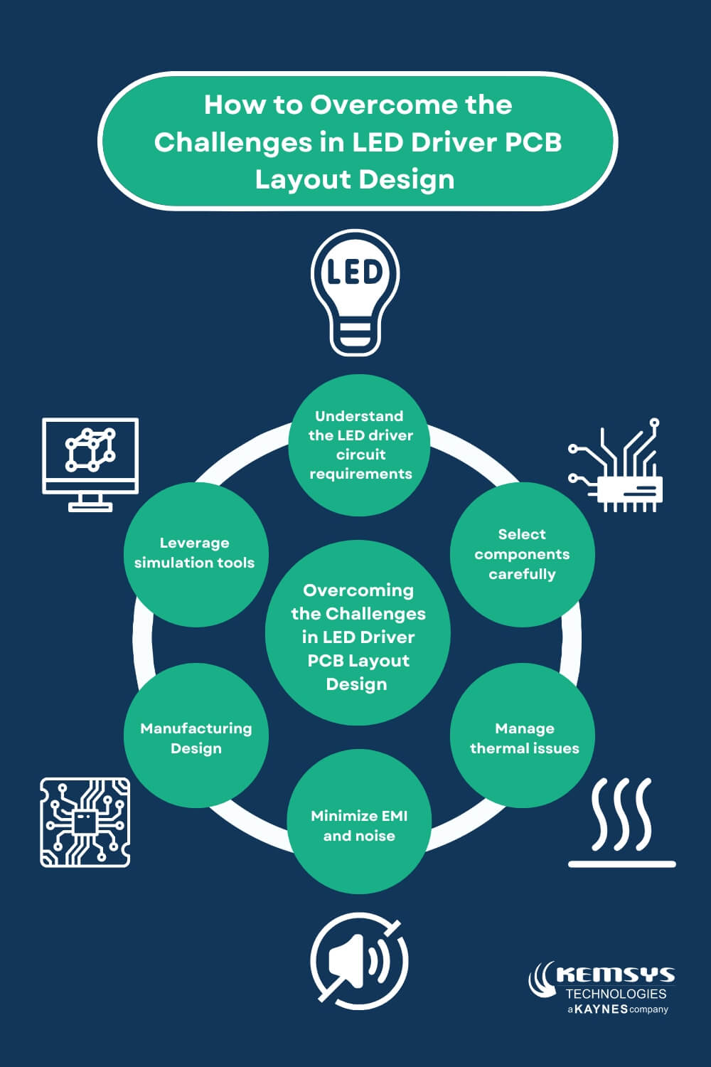
- Understand the LED Driver Circuit Requirements: Before starting the PCB layout design, it’s important to have a clear understanding of the LED driver circuit’s requirements, including voltage, current, and power ratings. This information will help guide component selection, layout design, and other aspects of the design process.
- Select Components Carefully: Selecting the right components for the LED driver circuit is critical to ensuring optimal performance and reliability. Choose components that meet the required specifications and are compatible with each other and be sure to consider factors such as thermal performance and EMI suppression.
- Manage Thermal Issues: Thermal management is critical for LED driver circuits, which can generate significant heat during operation. Strategies for managing thermal issues include using heat sinks, thermal vias, and proper PCB layout design to ensure optimal heat dissipation.
- Minimize EMI and Noise: EMI and noise can interfere with the operation of LED driver circuits. This can cause performance issues and potentially even damage the circuit. Best practices for minimizing EMI and noise include three things: proper grounding and shielding, careful component placement, and the use of EMI suppression techniques.
- Manufacturing design: PCB layout design should take into account the requirements of the manufacturing process. This includes considerations such as penalization, tooling holes, and proper spacing between components.
- Leverage Simulation Tools: Simulation tools such as SPICE models and PCB layout software can help to identify potential issues and optimize the design for performance, reliability, and efficiency.
By following these strategies and best practices, designers can overcome the challenges of LED driver PCB layout design and create high-quality, reliable LED lighting systems that operate effectively and efficiently.
Moving forward let’s discuss each of these considerations in detail. Let’s start with managing thermal issues in LED driver PCB layouts.
Understanding the LED Driver Circuit Requirements
Understanding the LED driver circuit requirements is a critical first step in successful PCB layout design for LED driver circuits. Some key considerations when understanding the LED driver circuit requirements include:
- Voltage Requirements: LED driver circuits must supply the correct voltage to the LED to ensure proper operation. This voltage may vary depending on the specific LED being used.
- Current Requirements: The circuits must provide the appropriate amount of current to the LED to ensure optimal performance and prevent damage. The required current may depend on factors such as the LED’s rated current and the desired brightness level.
- Power requirements: The designers must design LED driver circuits to handle the required power for the LED system. This may depend on factors such as the number of LEDs and the desired brightness level.
- Dimming Requirements: Designers must design the LED driver circuit to support the desired dimming range and response time if the LED system is dimmed.
- Efficiency Requirements: Designers should design the LED driver circuit with efficiency in mind to minimize energy consumption and reduce operating costs.
By understanding these LED driver circuit requirements, designers can select the appropriate components and design the PCB layout to meet the specific needs of the LED lighting system.
Strategies for Managing Thermal Issues in LED Driver PCB Layouts
Thermal management is a critical aspect of LED driver PCB layout design. Excessive heat can degrade component performance and reliability, leading to premature failure. Strategies for managing thermal issues in LED driver PCB layout includes –
Component Placement
The placement of components on the PCB can significantly impact thermal management. Designers should consider grouping heat-generating components together and placing them near heatsinks or areas with good airflow. Furthermore, to prevent heat buildup in specific areas of the PCB, designers should space out the components.
Heat Sinks
Designers commonly use heat sinks in LED driver PCB layouts to dissipate heat away from heat-generating components. When selecting a heat sink, designers should consider the size, material, and mounting method. Additionally, the heat sink should be in direct contact with the heat-generating component to maximize heat transfer.
Thermal Pads
Designers use thermal pads to transfer heat from a component to a heat sink or PCB. When selecting a thermal pad, designers should consider the material, thickness, and thermal conductivity. Furthermore, designers should ensure good thermal contact by applying the thermal pad with sufficient pressure. Making it large enough to cover the entire component.
Trace Width
The width of traces on the PCB can impact thermal management by affecting the amount of current that flows through them. When designing the PCB layout, designers should consider the maximum current and voltage requirements of the LED driver circuit. They should ensure that the trace width is sufficient to prevent excessive heat buildup.
Copper Pour
Designers use the copper pour technique in PCB layout design to increase thermal conductivity and heat dissipation. By pouring copper around heat-generating components, designers can improve thermal management and reduce the risk of component failure due to excessive heat.
PCB Material
The choice of PCB material can significantly impact thermal management. Although FR-4 is commonly used material for LED driver PCB layouts, designers can achieve better thermal conductivity and heat dissipation by using materials like aluminum and copper. Designers should consider the specific requirements of the LED driver circuit when selecting a PCB material.
Managing thermal issues in LED driver PCB layouts requires careful consideration of component placement, heat sinks, thermal pads, trace width, copper pour, and PCB material. By implementing these strategies, designers can ensure that their LED lighting systems are reliable, efficient, and have a longer lifespan.
Find out more on What is thermal management in LED driver design?
Minimizing EMI and Noise in LED Driver PCB Layouts: Best Practices
Electromagnetic interference (EMI) and noise can negatively impact the performance of LED driver circuits and the overall lighting system. Therefore, minimizing EMI and noise is critical in LED driver PCB layout design. Here are the best practices for minimizing EMI and noise in LED driver PCB layouts.
- Grounding: Proper grounding is essential for minimizing EMI and noise. Designers should make sure to connect all components to a ground plane that is as large as possible. Aditionally, designers should make sure that no other traces or components interrupt the ground plane.
- Component Placement: The placement of components can also impact EMI and noise. Designers should avoid placing high-speed components near sensitive analog components, as this can result in EMI and noise issues. Additionally, components should be placed away from the edges of the PCB to reduce the coupling of EMI.
- Filtering: The use of filtering components, such as capacitors and inductors, can help to reduce EMI and noise. Designers should place filtering components as close to the noise source as possible and use high-quality components with low ESR and ESL values.
- Shielding: Designers can use shielding techniques to reduce the coupling of EMI between components. They can enclose sensitive components or entire sections of the PCB using metal shields or conductive coatings. Designers should also shield cables and connectors to prevent EMI from entering or leaving the PCB.
- Trace Routing: Trace routing can also impact EMI and noise. Designers should route high-speed traces away from sensitive analog components and keep them as short as possible. Additionally, designers should avoid routing traces near edges or corners of the PCB, as this can result in increased EMI coupling.
- PCB Layout Design: The overall PCB layout design can also impact EMI and noise. Designers should follow best practices for power and ground routing. Such as using a star grounding scheme and minimizing the length of power and ground traces. Additionally, designers should optimize the PCB layout for EMI and noise by using techniques like differential signaling and impedance matching.
Reducing EMI and noise in LED driver PCBs requires careful design considerations including grounding, component placement, filtering, shielding, trace routing, and PCB layout. Implementing these best practices ensures high performance, reliability, and regulatory compliance for LED lighting systems.
Designing for Manufacturability: Tips for LED Driver PCB Layouts
Designing for manufacturability is critical in LED driver PCB layout design. It ensures that the final product can be efficiently and cost-effectively manufactured. Here are a few tips for designing LED driver PCB layouts for manufacturability.
Keep It Simple
Simplicity is key when designing for manufacturability. Designers should avoid complex layouts, which can result in errors during manufacturing and increase the cost of production. Components should be placed in a logical and straightforward manner, and the number of vias and layers should be minimized.
Design for Assembly
Designers should consider the assembly process when designing the PCB layout. Designers should place components in a way that allows for efficient assembly. They should provide easy access to solder joints and clear labeling of components. They should also use surface mount technology (SMT) components where possible, as machines can automatically place and solder them.
Use Standard Components
Using standard components can significantly reduce the cost of manufacturing. They are readily available and typically less expensive than custom components. Additionally, standard components can simplify the assembly process, as there is no need for special tooling or processes.
Test for Reliability
Testing for reliability during the design phase can help to reduce the risk of failure during production. Designers should conduct reliability testing, such as thermal and vibration testing. This ensures that the design can withstand the stresses of the manufacturing process and of the final product’s use.
Consider the PCB Fabrication Process
The PCB fabrication process can impact manufacturability. Designers should consider the manufacturing process when designing the PCB layout. They should focus on the minimum trace width and spacing, as well as the size and placement of drill holes. Designers should consider the type of solder mask and silkscreen used. These can impact the clarity of labeling and the quality of the final product.
Work with Experienced Manufacturers
Working with experienced PCB manufacturers can significantly improve manufacturability. Experienced manufacturers can provide guidance on PCB design for manufacturability. They can also offer advice on materials and production techniques that reduce costs and improve quality.
Designing LED driver PCB layouts for manufacturability requires careful consideration. This includes simplicity, design for assembly, standard components, reliability testing, the PCB fabrication process, and working with experienced manufacturers. By implementing these tips, designers can ensure that their LED lighting systems can be efficiently and cost-effectively manufactured. This results in a high-quality and reliable product.
Selecting Components for LED Driver PCB Layouts: Key Considerations
Choosing the right components is crucial for LED driver PCB layouts and impacts system performance and reliability.
Choosing the wrong components can lead to issues such as thermal runaway, component failure, and reduced efficiency. Let’s discuss the key considerations for selecting the components for LED driver PCB layouts.
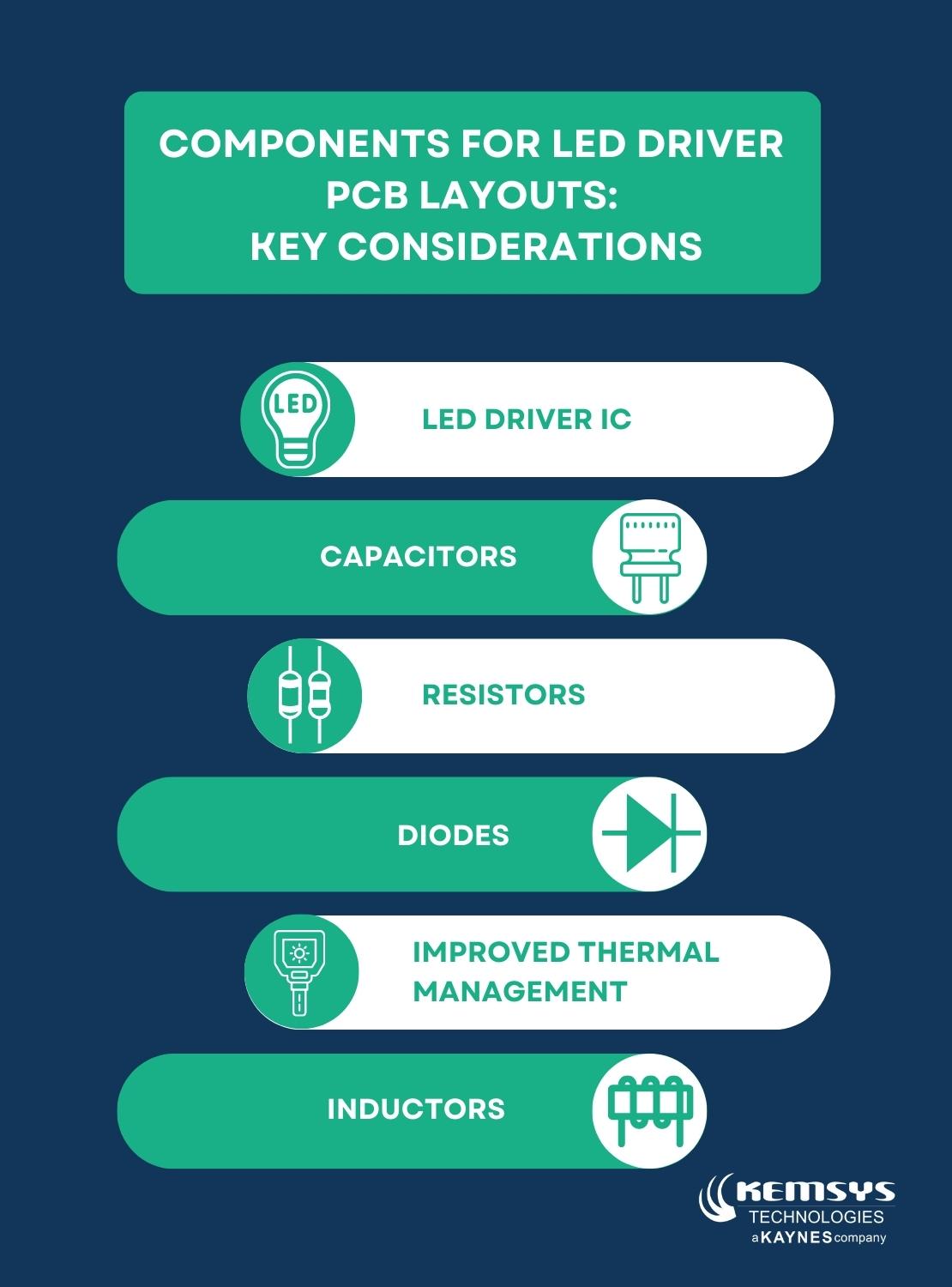
LED Driver ICs
The LED driver IC is the heart of the LED driver circuit and is responsible for regulating the current and voltage supplied to the LED. When selecting an LED driver IC, it is essential to consider the maximum current and voltage required by the LED, as well as the input voltage range of the driver circuit. Additionally, designers should look for ICs with built-in protection features such as overvoltage protection, overcurrent protection, and thermal protection.
Capacitors
Capacitors are essential components in LED driver circuits, as they help to filter noise and stabilize the voltage supplied to the LED. When selecting capacitors for LED driver PCB layouts, designers should consider the required capacitance, voltage rating, and temperature rating. Ceramic capacitors are commonly used in LED driver circuits due to their low cost and high capacitance, but designers should also consider other types of capacitors such as tantalum and aluminum electrolytic capacitors.
Resistors
Resistors are used in LED driver circuits to limit the current supplied to the LED and protect against overcurrent conditions. When selecting resistors, designers should consider the required resistance value and power rating. Surface-mount resistors are commonly used in LED driver PCB layouts due to their small size and low cost, but designers should also consider other types of resistors such as wirewound and metal film resistors for high-power applications.
Diodes
Diodes are used in LED driver circuits to protect against reverse current and voltage spikes. When selecting diodes for LED driver PCB layouts, designers should consider the maximum reverse voltage, maximum forward current, and reverse recovery time. Schottky diodes are commonly used in LED driver circuits due to their low forward voltage drop and fast switching speed, but designers should also consider other types of diodes such as Zener and TVS diodes for protection against voltage spikes.
Inductors
Inductors are used in LED driver circuits to filter noise and regulate current. When selecting inductors for LED driver PCB layouts, designers should consider the required inductance value, current rating, and resistance. Surface-mount inductors are commonly used in LED driver circuits due to their small size and high efficiency, but designers should also consider other types of inductors such as toroidal and ferrite core inductors for high-current and high-frequency applications.
MOSFETs
MOSFETs are used in LED driver circuits to switch the current supplied to the LED. When selecting MOSFETs for LED driver PCB layouts, designers should consider the maximum drain-source voltage, maximum drain current, and on-resistance. Power MOSFETs are commonly used in LED driver circuits due to their high efficiency and fast switching speed, but designers should also consider other types of MOSFETs such as insulated-gate bipolar transistors (IGBTs) for high-voltage applications.
Selecting components for LED driver PCB layouts requires careful consideration of factors such as maximum current and voltage requirements, input voltage range, protection features, and temperature ratings. By choosing the right components for the application, designers can ensure that their LED lighting systems are reliable, efficient, and cost-effective.
The Power of Simulation Tools for Successful LED Driver PCB Layout Design
Simulation tools are powerful resources that can help designers to optimize LED driver PCB layout design and ensure the success of their designs. These tools enable designers to model and simulate the performance of the LED driver circuit before it is physically constructed, allowing for adjustments to be made to the design to improve performance, reduce costs, and minimize risks. Here are a few factors that increase the value of simulation tools.
- Optimize Performance: Simulation tools allow designers to optimize the performance of the LED driver circuit by modeling and simulating different designs to determine which configuration provides the best results. This includes determining the optimal placement of components, adjusting the size and type of components, and optimizing the routing of the circuit to reduce interference and noise.
- Reduce Costs: Simulation tools can also help to reduce costs by allowing designers to test different components and configurations without the need for physical prototypes. This reduces the cost and time associated with building multiple prototypes and allows designers to make informed decisions about component selection and placement.
- Minimize Risks: Simulation tools can help to minimize risks associated with LED driver PCB layout design by allowing designers to identify potential issues and address them before the design is finalized. For example, simulation tools can identify potential thermal issues, noise and interference problems, and other issues that could impact the performance of the circuit or increase the risk of failure.
- Improve Time-to-Market: Simulation tools reduce need for physical prototypes & improve design testing, shortening time-to-market. Apart from that they optimize product performance, reliability, cost-effectiveness, and reduce development time and cost.
- Validate Design Assumptions: Simulation tools reduce risk of unexpected issues in final product by v alidating design assumptions before physical circuit construction. Simulation improves designer confidence and LED driver circuit quality and reliability.
Simulation tools are powerful resources that can greatly enhance the LED driver PCB layout design process. They enable designers to optimize performance, reduce costs, minimize risks, improve time-to-market, and validate design assumptions. By leveraging simulation tools, designers can create high-quality and reliable LED driver circuits that meet or exceed performance requirements and deliver exceptional value to their customers.
Wrapping Up
- Designing the PCB layout for LED driver circuits requires careful consideration of several key factors to ensure optimal performance, reliability, and efficiency.
- Understanding the requirements of the LED driver circuit, selecting the right components, managing thermal issues, minimizing EMI and noise, designing for manufacturability, and leveraging simulation tools are all critical considerations that must be addressed during the LED driver PCB layout design process.
- By following best practices and strategies for overcoming the challenges of LED driver PCB layout design, designers can create high-quality, reliable LED lighting systems that operate effectively and efficiently.
- With the continued growth of LED lighting technology, the importance of LED driver PCB layout design will only continue to increase, making it essential for designers to stay up to date with the latest techniques and technologies for successful LED driver PCB layout design.
